Try GOLD - Free
Is India's FAB VISION On Track Despite RECENT SETBACKS?
Electronics For You
|June 2025
Paused, not derailed—experts see the Adani and Zoho exits as distinct but strategic, not setbacks. Rather than failure, they signal a pivot: India’s chip drive now hinges on design depth and delivering existing models.

On April 30, 2025, reports emerged that the Adani Group had paused discussions with Israel’s Tower Semiconductor regarding a much-anticipated $10 billion chip fabrication model in India. A day later, software major Zoho announced the suspension of its $700 million plan to enter chip manufacturing.
The Economic Times framed these exits as a “setback to Prime Minister Narendra Modi, who has for several years tried to lure companies in his pursuit to make India a global chip manufacturing hub.”
Yet the reasons diverged. Zoho founder Sridhar Vembu explained that, despite an extensive search, the company could not secure a suitable technology partner to navigate the complexities of chipmaking. Adani, on the other hand, cited uncertainty around domestic demand and doubts over the model’s viability.
The shelving of two high-profile, capital-intensive ventures raises critical questions. What do these exits mean for India’s semiconductor roadmap—particularly as the domestic market is projected to reach $64 billion by 2026, and Union Electronics and IT Minister Ashwini Vaishnaw maintains that ‘Made-in-India’ chips will debut by year-end? Do these developments point to structural gaps in India’s readiness for chip manufacturing? Are policy frameworks overly optimistic—or are such shifts part of a natural evolution shaped by global headwinds?
A timeline
On September 6, 2024, Adani Group partnered with Israel’s Tower Semiconductor to establish a $10 billion semiconductor fabrication plant in Taloja, near Mumbai, maharashtra. Approved by the Maharashtra state government, the project was to be developed in two phases; the first with a production capacity of 40,000 semiconductor wafers per month, followed by expansion to 80,000 wafers per month in the second phase.
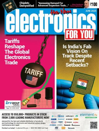

This story is from the June 2025 edition of Electronics For You.
Subscribe to Magzter GOLD to access thousands of curated premium stories, and 10,000+ magazines and newspapers.
Already a subscriber? Sign In
MORE STORIES FROM Electronics For You

Electronics For You
FM RADIO RECEIVER Using TDA7000
This FM radio receiver demonstrates the practical application of RF engineering and analogue signal-processing techniques.

4 mins
July 2026

Electronics For You
Latest 3D chip stacking method could extend Moore's Law
Engineered by a team at the University of Illinois Grainger College of Engineering in Urbana-Champaign, the process uses ultrathin single-crystalline silicon nanomembranes transferred at temperatures below 200°C, avoiding heat damage to underlying circuits.
1 min
July 2026

Electronics For You
Stretchable patch detects heart failure risks
Researchers at the University of Chicago's Pritzker School of Molecular Engineering in Chicago have developed an AI-powered stretchable computing patch capable of processing health data directly on the body in milliseconds, eliminating the need for external servers or wireless connections.
1 min
July 2026

Electronics For You
Simple 12V To 24V VOLTAGE DOUBLER
Many electronic circuits require a voltage higher than that available from the power supply.
3 mins
July 2026
Electronics For You
Crystal stress method reshapes nanochip manufacturing techniques
Research conducted at Rice University in Houston, Texas, demonstrated that alpha-molybdenum trioxide crystals can deform under an electron beam, generating highly ordered nanoscale wrinkles that function as optical gratings for guiding and manipulating light on chips.
1 min
July 2026

Electronics For You
Hidden Costs In IoT PRODUCT DEVELOPMENT
Hardware mistakes do not show up early in development. The most expensive hardware mistakes are rarely the obvious ones. Decisions made during design, testing, and architecture shape costs for years.
7 mins
July 2026

Electronics For You
Temperature-Based DUAL SAFETY SYSTEM For Smart Homes
A temperature-based dual safety system addresses common household risks through intelligent control.
4 mins
July 2026

Electronics For You
Smart material developed to fight counterfeiting
Engineered by a team at the Indian Institute of Technology Guwahati, the technology uses perovskite nanocrystals with a double-layer protective coating that improves resistance to heat and chemicals while maintaining optical performance.
1 min
July 2026

Electronics For You
President Murmu inaugurates semiconductor training fab at IISc
On June 3, 2026, President Droupadi Murmu inaugurated IISc Bengaluru’s Semiconductor Training Fab at CeNSE, established with support from the Ministry of Tribal Affairs.
4 mins
July 2026

Electronics For You
Quantum Li-Fi secures networks
Research conducted in Germany by a consortium led by KEEQuant and supported by Fraunhofer IPMS highlights a pathway toward flexible, high-security next-generation wireless networks.
1 min
July 2026
Listen
Translate
Change font size