Try GOLD - Free
FROM DESIGN TO MANUFACTURE: A Practical Guide To Faster Product Development
Electronics For You
|January 2026
Manufacturing has reached a point where speed and precision reinforce each other. Whether the focus is on an enclosure or a machined part, engineering teams now benefit from rapid validation and flexible production methods. When design decisions reflect how parts will ultimately be manufactured, development cycles shorten naturally.
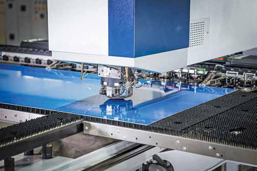
Across repeated engagements with product teams in enclosure engineering, sheet metal fabrication, 3D printing, and moulding, a clear pattern emerges: teams that embrace this pace iterate faster, reduce uncertainty, and move from prototype to production with greater confidence.
The opposite scenario is equally familiar. Strong ideas are often delayed not by manufacturing constraints, but by early design decisions that fail to align with real fabrication behaviour. This guide helps engineers avoid slowdowns and fully leverage the speed and clarity available in today's manufacturing environment.
Faster product development begins with a clearer intent
Most delays in mechanical product development do not originate on the shop floor. They begin upstream, when assumptions are made without fully considering the realities of forming, machining, moulding, or assembly.
Reversing this pattern is entirely achievable, and it begins with understanding. When engineers account for early in the design process how a bracket, frame, or enclosure will be built, the first prototype is much closer to the final product. This alignment can dramatically shorten development cycles.
Many enclosure designs appear flawless in CAD, yet include bends too close to holes, flanges without relief, or wall thicknesses that behave unpredictably during bending or machining. These are not failures but opportunities to refine. With small adjustments early in the design stage, such designs transition far more smoothly into fabrication.
Similarly, plastic enclosures intended for moulding behave differently when machined or 3D printed. Teams that anticipate these differences achieve clearer outcomes at every stage of development.
The key point is simple: these challenges are solved through awareness, not guesswork.
Choosing the right process unlocks speed


This story is from the January 2026 edition of Electronics For You.
Subscribe to Magzter GOLD to access thousands of curated premium stories, and 10,000+ magazines and newspapers.
Already a subscriber? Sign In
MORE STORIES FROM Electronics For You

Electronics For You
FM RADIO RECEIVER Using TDA7000
This FM radio receiver demonstrates the practical application of RF engineering and analogue signal-processing techniques.

4 mins
July 2026

Electronics For You
Latest 3D chip stacking method could extend Moore's Law
Engineered by a team at the University of Illinois Grainger College of Engineering in Urbana-Champaign, the process uses ultrathin single-crystalline silicon nanomembranes transferred at temperatures below 200°C, avoiding heat damage to underlying circuits.
1 min
July 2026

Electronics For You
Stretchable patch detects heart failure risks
Researchers at the University of Chicago's Pritzker School of Molecular Engineering in Chicago have developed an AI-powered stretchable computing patch capable of processing health data directly on the body in milliseconds, eliminating the need for external servers or wireless connections.
1 min
July 2026

Electronics For You
Simple 12V To 24V VOLTAGE DOUBLER
Many electronic circuits require a voltage higher than that available from the power supply.
3 mins
July 2026
Electronics For You
Crystal stress method reshapes nanochip manufacturing techniques
Research conducted at Rice University in Houston, Texas, demonstrated that alpha-molybdenum trioxide crystals can deform under an electron beam, generating highly ordered nanoscale wrinkles that function as optical gratings for guiding and manipulating light on chips.
1 min
July 2026

Electronics For You
Hidden Costs In IoT PRODUCT DEVELOPMENT
Hardware mistakes do not show up early in development. The most expensive hardware mistakes are rarely the obvious ones. Decisions made during design, testing, and architecture shape costs for years.
7 mins
July 2026

Electronics For You
Temperature-Based DUAL SAFETY SYSTEM For Smart Homes
A temperature-based dual safety system addresses common household risks through intelligent control.
4 mins
July 2026

Electronics For You
Smart material developed to fight counterfeiting
Engineered by a team at the Indian Institute of Technology Guwahati, the technology uses perovskite nanocrystals with a double-layer protective coating that improves resistance to heat and chemicals while maintaining optical performance.
1 min
July 2026

Electronics For You
President Murmu inaugurates semiconductor training fab at IISc
On June 3, 2026, President Droupadi Murmu inaugurated IISc Bengaluru’s Semiconductor Training Fab at CeNSE, established with support from the Ministry of Tribal Affairs.
4 mins
July 2026

Electronics For You
Quantum Li-Fi secures networks
Research conducted in Germany by a consortium led by KEEQuant and supported by Fraunhofer IPMS highlights a pathway toward flexible, high-security next-generation wireless networks.
1 min
July 2026
Listen
Translate
Change font size