Try GOLD - Free
Nodes Above 28nm Should Enter Commercial Production By 2028, 28nm Expected By 2029
Electronics For You
|July 2026
Launched in 2021 and operationalised in 2022, the India Semiconductor Mission (ISM) is driving India's ambition to build a self-reliant semiconductor ecosystem spanning manufacturing, design, talent, and supply chains. In this exclusive interview, Dr Satya Gupta, President of the VLSI Society of India (VSI), speaks with Shri Amitesh Kumar Sinha, Additional Secretary, MeitY, and CEO of ISM, about the mission's progress, challenges, and roadmap for India's semiconductor future.
-
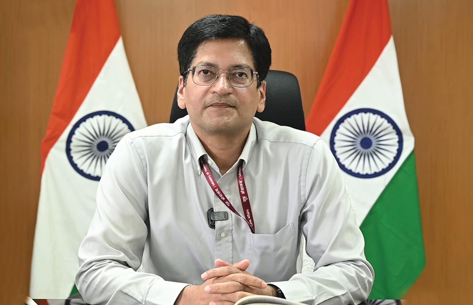
You have been associated with the ISM since its inception. Looking back over the past four-and-a-half years, how would you assess its progress, achievements, and key challenges?
The Union Cabinet approved the India Semiconductor Policy and the ISM on 15th December 2021, marking India's first comprehensive semiconductor policy backed by a long-term vision and strong commitment from Prime Minister Shri Narendra Modi and the Union Minister of Electronics and Information Technology, Shri Ashwini Vaishnaw.
Our biggest challenge at the outset was the absence of a semiconductor ecosystem. Without one, attracting global manufacturers is extremely difficult. The first proposals we received were not sufficiently convincing, and because semiconductor manufacturing is highly complex, particularly for a first-time entrant like India, we approved only those projects with a high probability of success.
To ensure this, we established rigorous evaluation criteria and constituted committees of global techno-commercial experts. Every project had to satisfy three nonnegotiable requirements:
• Strong financing. Applicants needed deep financial strength backed by profitable or cash-rich parent companies capable of withstanding the cyclical nature of the semiconductor industry. Many early applicants were attracted primarily by government incentives, so identifying genuinely committed partners took time.
• Credible technology transfer. We required complete production-ready technology transfer rather than simple licensing agreements. This included equipment specifications, workforce training, utility planning, installation support, prototype wafer runs, and qualification processes.
• Customer off-take. Technology partners had to commit production and bring established customers, giving global buyers confidence in India’s new manufacturing facilities.
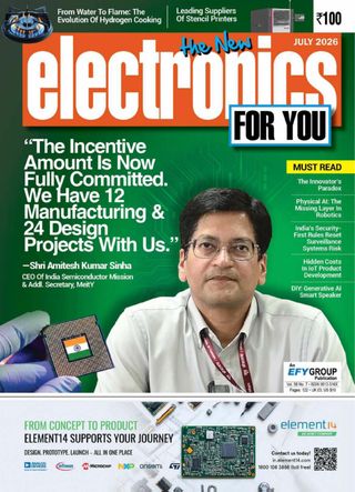

This story is from the July 2026 edition of Electronics For You.
Subscribe to Magzter GOLD to access thousands of curated premium stories, and 10,000+ magazines and newspapers.
Already a subscriber? Sign In
MORE STORIES FROM Electronics For You

Electronics For You
FM RADIO RECEIVER Using TDA7000
This FM radio receiver demonstrates the practical application of RF engineering and analogue signal-processing techniques.

4 mins
July 2026

Electronics For You
Latest 3D chip stacking method could extend Moore's Law
Engineered by a team at the University of Illinois Grainger College of Engineering in Urbana-Champaign, the process uses ultrathin single-crystalline silicon nanomembranes transferred at temperatures below 200°C, avoiding heat damage to underlying circuits.
1 min
July 2026

Electronics For You
Stretchable patch detects heart failure risks
Researchers at the University of Chicago's Pritzker School of Molecular Engineering in Chicago have developed an AI-powered stretchable computing patch capable of processing health data directly on the body in milliseconds, eliminating the need for external servers or wireless connections.
1 min
July 2026

Electronics For You
Simple 12V To 24V VOLTAGE DOUBLER
Many electronic circuits require a voltage higher than that available from the power supply.
3 mins
July 2026
Electronics For You
Crystal stress method reshapes nanochip manufacturing techniques
Research conducted at Rice University in Houston, Texas, demonstrated that alpha-molybdenum trioxide crystals can deform under an electron beam, generating highly ordered nanoscale wrinkles that function as optical gratings for guiding and manipulating light on chips.
1 min
July 2026

Electronics For You
Hidden Costs In IoT PRODUCT DEVELOPMENT
Hardware mistakes do not show up early in development. The most expensive hardware mistakes are rarely the obvious ones. Decisions made during design, testing, and architecture shape costs for years.
7 mins
July 2026

Electronics For You
Temperature-Based DUAL SAFETY SYSTEM For Smart Homes
A temperature-based dual safety system addresses common household risks through intelligent control.
4 mins
July 2026
Electronics For You
Smart material developed to fight counterfeiting
Engineered by a team at the Indian Institute of Technology Guwahati, the technology uses perovskite nanocrystals with a double-layer protective coating that improves resistance to heat and chemicals while maintaining optical performance.
1 min
July 2026

Electronics For You
President Murmu inaugurates semiconductor training fab at IISc
On June 3, 2026, President Droupadi Murmu inaugurated IISc Bengaluru’s Semiconductor Training Fab at CeNSE, established with support from the Ministry of Tribal Affairs.
4 mins
July 2026

Electronics For You
Quantum Li-Fi secures networks
Research conducted in Germany by a consortium led by KEEQuant and supported by Fraunhofer IPMS highlights a pathway toward flexible, high-security next-generation wireless networks.
1 min
July 2026
Listen
Translate
Change font size