Try GOLD - Free
"THE CZOCHRALSKI METHOD Is Preferred For Wafers Over 203mm"
Electronics For You
|November 2025
How are large-diameter silicon wafers produced, and why does the Czochralski technique remain the industry's choice? Rajasekar Elavarasan of Raana Semiconductors explains to EFY's Nitisha Dubey how this method ensures the crystal precision essential for advanced IC fabrication.
-

Which technique is essential for manufacturing silicon wafers?
The Czochralski technique is the standard process for producing silicon ingots used in wafer manufacturing. The process begins with polysilicon as the raw material. Polysilicon is melted in a crucible at about 1500°C. A seed crystal is then dipped into the molten silicon and slowly pulled upward, allowing the material to solidify into a single-crystal ingot. These ingots, typically 300mm in diameter and up to 3-metres long, are then cut, lapped, and polished to form silicon wafers. These wafers serve as substrates for microelectronic-grade IC fabrication, a process crucial to the production of modern electronic components.
Why is the Czochralski method preferred for producing silicon wafers?
The Czochralski method dominates large wafer production because it can produce silicon ingots exceeding 203mm (8-inches) in diameter, unlike the Bridgman or float-zone methods, which are limited to smaller sizes.
What are the key techniques for producing advanced semiconductors?


This story is from the November 2025 edition of Electronics For You.
Subscribe to Magzter GOLD to access thousands of curated premium stories, and 10,000+ magazines and newspapers.
Already a subscriber? Sign In
MORE STORIES FROM Electronics For You

Electronics For You
FM RADIO RECEIVER Using TDA7000
This FM radio receiver demonstrates the practical application of RF engineering and analogue signal-processing techniques.

4 mins
July 2026
Electronics For You
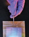
Latest 3D chip stacking method could extend Moore's Law
Engineered by a team at the University of Illinois Grainger College of Engineering in Urbana-Champaign, the process uses ultrathin single-crystalline silicon nanomembranes transferred at temperatures below 200°C, avoiding heat damage to underlying circuits.
1 min
July 2026
Electronics For You
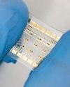
Stretchable patch detects heart failure risks
Researchers at the University of Chicago's Pritzker School of Molecular Engineering in Chicago have developed an AI-powered stretchable computing patch capable of processing health data directly on the body in milliseconds, eliminating the need for external servers or wireless connections.
1 min
July 2026

Electronics For You
Simple 12V To 24V VOLTAGE DOUBLER
Many electronic circuits require a voltage higher than that available from the power supply.
3 mins
July 2026
Electronics For You
Crystal stress method reshapes nanochip manufacturing techniques
Research conducted at Rice University in Houston, Texas, demonstrated that alpha-molybdenum trioxide crystals can deform under an electron beam, generating highly ordered nanoscale wrinkles that function as optical gratings for guiding and manipulating light on chips.
1 min
July 2026

Electronics For You
Hidden Costs In IoT PRODUCT DEVELOPMENT
Hardware mistakes do not show up early in development. The most expensive hardware mistakes are rarely the obvious ones. Decisions made during design, testing, and architecture shape costs for years.
7 mins
July 2026

Electronics For You
Temperature-Based DUAL SAFETY SYSTEM For Smart Homes
A temperature-based dual safety system addresses common household risks through intelligent control.
4 mins
July 2026
Electronics For You
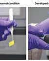
Smart material developed to fight counterfeiting
Engineered by a team at the Indian Institute of Technology Guwahati, the technology uses perovskite nanocrystals with a double-layer protective coating that improves resistance to heat and chemicals while maintaining optical performance.
1 min
July 2026

Electronics For You
President Murmu inaugurates semiconductor training fab at IISc
On June 3, 2026, President Droupadi Murmu inaugurated IISc Bengaluru’s Semiconductor Training Fab at CeNSE, established with support from the Ministry of Tribal Affairs.
4 mins
July 2026

Electronics For You
Quantum Li-Fi secures networks
Research conducted in Germany by a consortium led by KEEQuant and supported by Fraunhofer IPMS highlights a pathway toward flexible, high-security next-generation wireless networks.
1 min
July 2026
Listen
Translate
Change font size