Prova GOLD - Gratis
Simple Tricks To Pack MORE 5G ANTENNAS
Electronics For You
|March 2026
Can compact isolation structures enable denser 5G antennas? PCB-friendly isolation techniques make it possible to place more antennas into tight layouts without sacrificing isolation, gain, or efficiency.
-
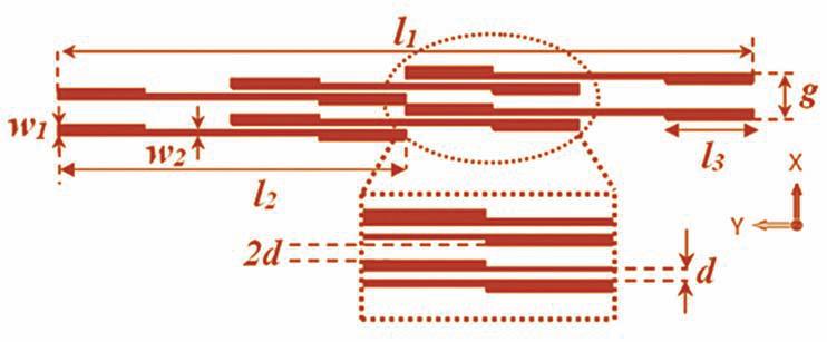
Designers of 5G radios face a constant squeeze: product teams demand more antennas in less space to support higher capacity, beamforming, and MIMO, while RF physics penalises elements placed too close together. As spacing shrinks, mutual coupling quietly degrades matching, distorts radiation patterns, and reduces array efficiency.
Across antenna research and consulting projects for 3.5GHz 5G systems, the outcome often depends on how effectively coupling is controlled within just a few millimetres of PCB space. Small layout decisions in this narrow gap frequently determine whether an array performs reliably or falls short.
Compact isolation structures, such as parallel-coupled line resonators and carefully shaped ground features, provide a practical way to increase antenna density in 5G and future systems. These solutions fill the limited gaps already available, use standard PCB processes, and deliver measurable isolation improvements in real hardware.
Why spacing alone is not enough
The simplest way to reduce coupling is to increase the distance between elements. For many 5G arrays at 3.5GHz, designers aim for element spacings around half a wavelength. That approach works until mechanical constraints, size limitations, and multi-band packaging push antennas closer together.
Once you move below these comfortable spacings, following happens:
• Surface waves on the substrate become a significant coupling path.
• The input impedance of each element changes due to its neighbours.
• Radiation patterns and front-to-back ratio degrade, directly impacting coverage and MIMO performance.
In consulting work, I have seen arrays that simulated well as isolated elements but failed in the final product because real-world spacing and housing forced much tighter layouts. At that point, we can no longer 'buy' isolation with space; we must engineer the coupling path itself.


Den här artikeln är från utgåvan March 2026 av Electronics For You.
Prenumerera på Magzter GOLD för att få tillgång till tusentals kurerade premiumartiklar samt 10 000+ tidskrifter och dagstidningar.
Redan prenumerant? Logga in
FLER ARTIKLAR FRÅN Electronics For You

Electronics For You
FM RADIO RECEIVER Using TDA7000
This FM radio receiver demonstrates the practical application of RF engineering and analogue signal-processing techniques.

4 mins
July 2026

Electronics For You
Latest 3D chip stacking method could extend Moore's Law
Engineered by a team at the University of Illinois Grainger College of Engineering in Urbana-Champaign, the process uses ultrathin single-crystalline silicon nanomembranes transferred at temperatures below 200°C, avoiding heat damage to underlying circuits.
1 min
July 2026

Electronics For You
Stretchable patch detects heart failure risks
Researchers at the University of Chicago's Pritzker School of Molecular Engineering in Chicago have developed an AI-powered stretchable computing patch capable of processing health data directly on the body in milliseconds, eliminating the need for external servers or wireless connections.
1 min
July 2026

Electronics For You
Simple 12V To 24V VOLTAGE DOUBLER
Many electronic circuits require a voltage higher than that available from the power supply.
3 mins
July 2026
Electronics For You
Crystal stress method reshapes nanochip manufacturing techniques
Research conducted at Rice University in Houston, Texas, demonstrated that alpha-molybdenum trioxide crystals can deform under an electron beam, generating highly ordered nanoscale wrinkles that function as optical gratings for guiding and manipulating light on chips.
1 min
July 2026

Electronics For You
Hidden Costs In IoT PRODUCT DEVELOPMENT
Hardware mistakes do not show up early in development. The most expensive hardware mistakes are rarely the obvious ones. Decisions made during design, testing, and architecture shape costs for years.
7 mins
July 2026

Electronics For You
Temperature-Based DUAL SAFETY SYSTEM For Smart Homes
A temperature-based dual safety system addresses common household risks through intelligent control.
4 mins
July 2026

Electronics For You
Smart material developed to fight counterfeiting
Engineered by a team at the Indian Institute of Technology Guwahati, the technology uses perovskite nanocrystals with a double-layer protective coating that improves resistance to heat and chemicals while maintaining optical performance.
1 min
July 2026

Electronics For You
President Murmu inaugurates semiconductor training fab at IISc
On June 3, 2026, President Droupadi Murmu inaugurated IISc Bengaluru’s Semiconductor Training Fab at CeNSE, established with support from the Ministry of Tribal Affairs.
4 mins
July 2026

Electronics For You
Quantum Li-Fi secures networks
Research conducted in Germany by a consortium led by KEEQuant and supported by Fraunhofer IPMS highlights a pathway toward flexible, high-security next-generation wireless networks.
1 min
July 2026
Listen
Translate
Change font size